Ideal Vacuum Circular Magnetron Sputtering Targets, MOLYBDENUM - Mo Sputtering Target, 3'' Diameter x 0.25" Thick, 99.95 % Percent Purity
Ideal Vacuum Products, LLC.
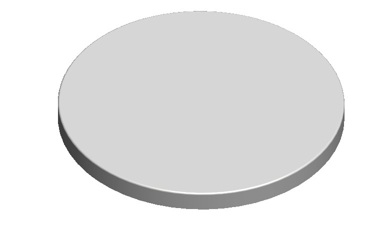
This product is a circular magnetron Molybdenum - Mo sputtering target, with a 3'' diameter x 0.25" thickness. It is 99.95% pure.
We use a very competitive pricing strategy to ensure you receive the highest quality products at the best possible value, giving you both affordability and excellence in every purchase. We offer huge discounts to every customer, customers who place bulk orders will enjoy huge savings. We stock huge quantities of our products to give our customers guaranteed same day shipping after placing an order. This short lead time is loved by all our customers who look to manage their cash flow with quicker turnaround times. Our regular customers can maintain lower inventory levels, decreasing storage costs and minimizing the risk of obsolescence. Buying from Ideal Vacuum means a customer receives their product more quickly, enhancing satisfaction and meeting their urgent needs. This also enables our customers to stay ahead of their competition by quickly adapting to new trends and demands.
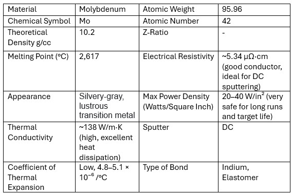
MOLYBDENUM (Mo)
Key Properties
Appearance: Silvery-gray, lustrous transition metal
Density: ~10.22 g/cm³
Crystal Structure: Body-centered cubic (BCC)
Melting Point: 2623 °C (very high thermal stability)
Boiling Point: ~4639 °C
Thermal Conductivity: ~138 W/m·K (high, excellent heat dissipation)
Electrical Resistivity: ~5.34 µO·cm (good conductor, ideal for DC sputtering)
Chemical Stability: Good corrosion resistance; forms a stable oxide (MoO3) in air at elevated temperatures
Sputtering Behavior: High melting point and good thermal conductivity allow high power densities without damage; sputters cleanly with DC or pulsed DC power
Key Applications:
Molybdenum is a widely used target material in PVD sputtering for producing films with excellent conductivity, adhesion, and stability.
Semiconductor Metallization: Gate and interconnect layers in TFTs and other devices
Transparent Conductive Oxide (TCO) Back Contacts: Mo layers under CIGS solar cells for adhesion and conductivity
Barrier Layers: Diffusion barriers in microelectronics (e.g., preventing Cu migration)
Reflective & Optical Coatings: High reflectivity in infrared, used in thermal mirrors and IR optics
Hard & Wear-Resistant Coatings: Protective metallic layers in mechanical components
Adhesion Layers: Promotes adhesion between ceramics, semiconductors, and other metals in multilayer stacks
Summary
Molybdenums high melting point, excellent thermal/electrical conductivity, and chemical stability make it a robust and versatile thin film material for electronics, photovoltaics, optics, and protective coatings in PVD applications.
 Notes:
Metallic or elastomer backing plate bonding is recommended for all dielectric target materials because these materials have characteristics which are not amenable to sputtering, such as, brittleness and low thermal conductivity. These targets are most susceptible to thermal shock due to their low thermal conductivity and hence, may require specific power ramp up and ramp down procedures during start up and shut down steps.