Ideal Vacuum Circular Magnetron Sputtering Targets, COPPER - Cu Sputtering Target or Cu Backing Plate, 3'' Diameter x 0.25" Thick, 99.99 Percent Purity
Ideal Vacuum Products, LLC.
This product is a circular magnetron COPPER - Cu sputtering target, or Cu backing plate, with a 3'' diameter x 0.25" thickness. It is 99.99% pure.
We use a very competitive pricing strategy to ensure you receive the highest quality products at the best possible value, giving you both affordability and excellence in every purchase. We offer huge discounts to every customer, customers who place bulk orders will enjoy huge savings. We stock huge quantities of our products to give our customers guaranteed same day shipping after placing an order. This short lead time is loved by all our customers who look to manage their cash flow with quicker turnaround times. Our regular customers can maintain lower inventory levels, decreasing storage costs and minimizing the risk of obsolescence. Buying from Ideal Vacuum means a customer receives their product more quickly, enhancing satisfaction and meeting their urgent needs. This also enables our customers to stay ahead of their competition by quickly adapting to new trends and demands.
COPPER - Cu
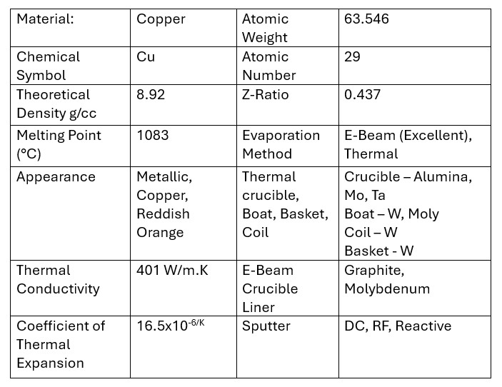
Copper (Cu) sputtering targets are commonly used in thin-film deposition due to copper’s excellent electrical and thermal properties. Here’s a concise summary of copper sputtering targets in thin films:
1. Material Properties:
High Electrical Conductivity: Copper is one of the best conductors of electricity, making it ideal for thin films in microelectronics and electrical applications.
Thermal Conductivity: Copper has high thermal conductivity, making it valuable for thin films where heat dissipation is critical.
Ductility: Copper is a ductile material, meaning it can form thin films that are mechanically stable and flexible.
2. Deposition Methods:
DC Sputtering: Since copper is a conductive material, DC magnetron sputtering is commonly used for efficient thin-film deposition.
RF Sputtering: Although DC sputtering is preferred, RF sputtering can also be used for certain applications where alternating fields are necessary.
Reactive Sputtering: Copper can be sputtered in reactive environments with gases like oxygen to form copper oxides (e.g., CuO, Cu2O) for specific applications.
3. Applications:
Microelectronics: Copper is extensively used in integrated circuits, semiconductor devices, and thin-film transistors as interconnects and electrical contacts due to its superior electrical conductivity.
Printed Circuit Boards (PCBs): Thin films of copper are crucial in the manufacture of PCBs, where they form conductive pathways for electronic components.
Solar Cells: Copper is used in some thin-film solar cells for electrical contacts and as a component in compounds like CIGS (copper indium gallium selenide).
Optical Coatings: Copper is occasionally used in reflective coatings and mirrors due to its high reflectivity in the visible and infrared ranges.
Heat Sinks and Thermal Management: Copper thin films are used in applications where thermal conductivity is essential, such as heat sinks and thermal management layers in microelectronics.
4. Film Properties:
High Electrical Conductivity: Copper thin films have excellent electrical properties, making them ideal for conductive layers in electronics.
Thermal Conductivity: Copper films efficiently dissipate heat, improving device reliability and longevity in high-power electronic applications.
Corrosion Resistance: Copper films can be susceptible to oxidation, so protective layers (like nickel or chromium) are often added to prevent corrosion.
Adhesion: Copper has good adhesion to a variety of substrates, but adhesion layers (like titanium or chromium) are sometimes used to enhance bonding with certain materials.
5. Reactive Deposition:
Copper Oxides (CuO, Cu2O): Copper can be sputtered in an oxygen-rich environment to form copper oxides, which have applications in electronics, sensors, and photovoltaics due to their semiconducting properties.
6. Challenges:
Oxidation: Copper is prone to oxidation, especially in the presence of air or moisture. To avoid this, deposition is often done in a controlled environment, and additional protective layers may be applied.
Electromigration: In microelectronics, thin copper films can experience electromigration, where atoms move under the influence of an electrical current, potentially leading to device failure. Barrier layers (e.g., tantalum or titanium) are used to mitigate this effect.
Diffusion: Copper can diffuse into other materials, particularly silicon, which can degrade device performance. Diffusion barriers (like tantalum) are used to prevent this.
Summary:
Copper (Cu) sputtering targets are essential for thin-film applications in microelectronics, solar cells, optical coatings, and thermal management due to copper’s high electrical conductivity, thermal conductivity, and ductility. DC sputtering is commonly used for copper deposition, and reactive sputtering can create copper oxides for specialized applications. Copper thin films are widely used for interconnects, electrical contacts, and heat dissipation, though care must be taken to prevent oxidation and diffusion in sensitive applications.

 Notes:
Metallic or elastomer backing plate bonding is recommended for all dielectric target materials because these materials have characteristics which are not amenable to sputtering, such as, brittleness and low thermal conductivity. These targets are most susceptible to thermal shock due to their low thermal conductivity and hence, may require specific power ramp up and ramp down procedures during start up and shut down steps.
|