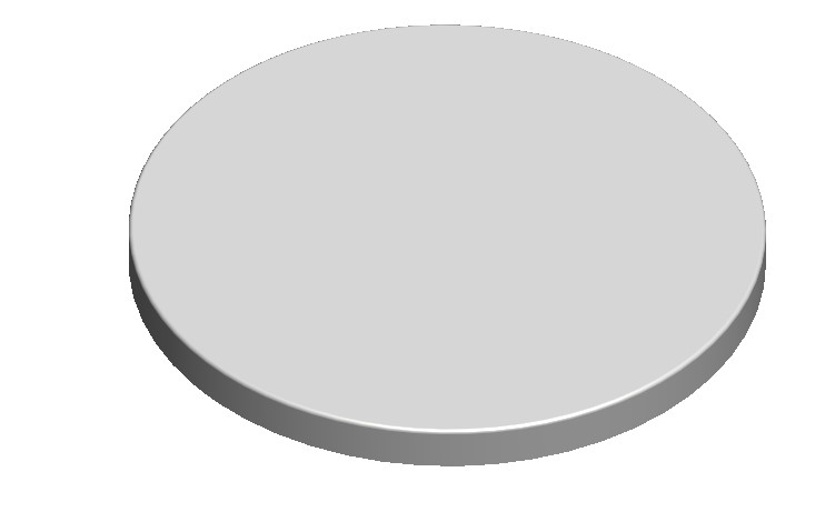
Ideal Vacuum Circular Magnetron Sputtering Targets, NIOBIUM - Nb Sputtering Target, 3'' Diameter x 0.25" Thick, 99.95 Percent Purity.
Ideal Vacuum Products, LLC.
This product is a circular magnetron NIOBIUM - Nb sputtering target, with a 3'' diameter x 0.25" thickness. It is 99.95% pure.
We use a very competitive pricing strategy to ensure you receive the highest quality products at the best possible value, giving you both affordability and excellence in every purchase. We offer huge discounts to every customer, customers who place bulk orders will enjoy huge savings. We stock huge quantities of our products to give our customers guaranteed same day shipping after placing an order. This short lead time is loved by all our customers who look to manage their cash flow with quicker turnaround times. Our regular customers can maintain lower inventory levels, decreasing storage costs and minimizing the risk of obsolescence. Buying from Ideal Vacuum means a customer receives their product more quickly, enhancing satisfaction and meeting their urgent needs. This also enables our customers to stay ahead of their competition by quickly adapting to new trends and demands.
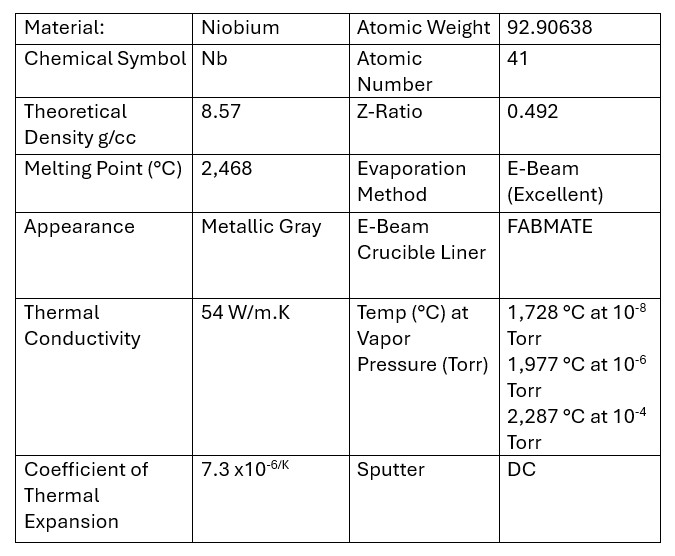
NIOBIUM - Nb
Niobium (Nb) sputtering targets are widely used in thin-film deposition due to niobium�s unique electrical, mechanical, and superconducting properties. Here�s a concise summary of niobium sputtering targets in thin films:
1. Material Properties:
High Melting Point: Niobium has a high melting point (~2477�C), making it suitable for high-temperature applications.
Corrosion Resistance: Niobium is resistant to oxidation and corrosion, especially in acidic environments.
Superconductivity: Niobium is a key material in superconducting applications, particularly for its high critical temperature (Tc) and ability to carry large superconducting currents.
Electrical Conductivity: Niobium is a conductive material, making it useful in electronic and electrical thin-film applications.
2. Deposition Methods:
DC Sputtering: Since niobium is conductive, DC magnetron sputtering is commonly used, offering efficient deposition rates.
RF Sputtering: RF sputtering may be used for specialized applications or in conjunction with reactive sputtering to form niobium compounds.
Reactive Sputtering: Niobium can be sputtered in a reactive atmosphere (e.g., with oxygen or nitrogen) to form niobium oxide (Nb2O5) or niobium nitride (NbN) for specific applications.
3. Applications:
Superconducting Films: Niobium is a key material in superconducting films, which are used in superconducting quantum interference devices (SQUIDs), superconducting circuits, and particle accelerators.
Microelectronics: Niobium thin films are used in capacitors, interconnects, and as diffusion barriers in microelectronics due to their excellent conductivity and stability.
Optical Coatings: Niobium is used in reflective coatings and optical filters. Reactive sputtering forms niobium pentoxide (Nb2O5), which is used in high-index optical coatings.
Protective Coatings: Niobium�s corrosion and oxidation resistance make it useful for protective coatings in chemical processing and high-performance applications.
Niobium Nitride (NbN): Formed via reactive sputtering, NbN is used in superconducting films, hard coatings, and wear-resistant layers.
4. Film Properties:
Superconductivity: Niobium thin films exhibit superconductivity at low temperatures, making them essential in quantum computing and high-performance superconducting circuits.
Corrosion Resistance: Niobium films provide excellent protection against corrosion, particularly in aggressive environments, making them useful for protective and barrier layers.
Optical Properties: Niobium oxide (Nb2O5) films have a high refractive index (~2.2) and are used in optical coatings.
Mechanical Strength: Niobium films are strong and durable, making them suitable for applications where wear resistance is needed.
5. Reactive Deposition:
Niobium Pentoxide (Nb2O5): Formed through reactive sputtering with oxygen, Nb2O5 is used in optical coatings, dielectrics, and capacitors due to its high dielectric constant and optical transparency.
Niobium Nitride (NbN): NbN films are used in superconducting applications, as well as in hard coatings for cutting tools and wear-resistant surfaces.
6. Challenges:
Target Poisoning: In reactive sputtering, target poisoning can occur, where non-metallic compounds (e.g., oxides or nitrides) form on the target, reducing the sputtering efficiency.
Internal Stress: Niobium films can develop internal stress during deposition, which can affect the mechanical properties and adhesion of the film.
Summary:
Niobium (Nb) sputtering targets are widely used in thin films for applications in superconductivity, microelectronics, optical coatings, and protective layers. DC sputtering is commonly used to deposit niobium thin films, while reactive sputtering is used to form niobium compounds like Nb2O5 (optical coatings, dielectrics) and NbN (superconducting films, hard coatings). Niobium thin films are valued for their superconducting properties, corrosion resistance, and mechanical durability across various industries.
 Notes:
Metallic or elastomer backing plate bonding is recommended for all dielectric target materials because these materials have characteristics which are not amenable to sputtering, such as, brittleness and low thermal conductivity. These targets are most susceptible to thermal shock due to their low thermal conductivity and hence, may require specific power ramp up and ramp down procedures during start up and shut down steps.
|


